已發表 :11/9/2020 上午3:28:18
點擊計數:2103
In the past ten years, various computing workloads have developed rapidly, but Moore's Law has been repeatedly rumored to come to an end. Facing the demands of more diversified computing applications, in order to "plug" more functions into the same chip, advanced packaging technology has become a key innovation path to continuously optimize chip performance and cost.
TSMC, Intel, and Samsung are all accelerating the deployment of 3D packaging technology. In August of this year, the three major chip manufacturing giants all showed up, making the battlefield more and more smoke.
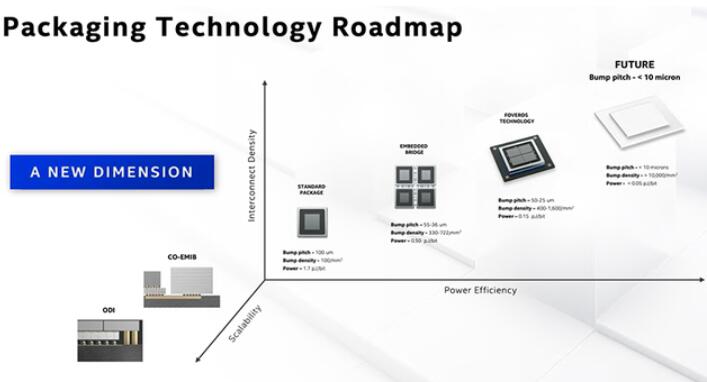
▲Intel Packaging Technology Roadmap
Through the advanced packaging layout of the three major chip manufacturing giants, we can see that in the next year, 3D packaging technology will be an important killer beyond Moore's Law.
1. Advanced packaging: squeeze more functions into one chip
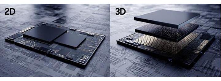
Previously, chips mostly used 2D planar packaging technology. However, with the increasing demand for heterogeneous computing applications, 3D packaging technology that can integrate chips of different sizes, different manufacturing processes, and different materials has become a combination of higher performance and higher flexibility. The necessary choice for sex.
From the perspective of the latest 3D packaging technology landing progress, Intel Lakefield uses 3D packaging technology Foveros, TSMC’s 3D packaging technology SoIC will be mass-produced in 2021 as originally planned, and Samsung’s 3D packaging technology has been applied to 7nm EUV chips.
Why move towards advanced packaging technology? There are two main reasons. One is that most of the performance limitations of processors so far come from memory bandwidth, and the other is productivity increases.
On the one hand, the development speed of storage bandwidth is much lower than the speed of the processor logic circuit, so there is a "memory wall" problem.
In traditional PCB packaging, it is difficult to increase the trace density and signal transmission rate, so the memory bandwidth increases slowly. The trace density of advanced packaging is short, the signal transmission rate has a lot of room for improvement, and the interconnection density can be greatly improved, so advanced packaging technology has become one of the main methods to solve the memory wall problem.
On the other hand, the architecture of high-performance processors is becoming more and more complex, and the number of transistors is also increasing, but advanced semiconductor processes are still expensive and the productivity is not satisfactory.
In semiconductor manufacturing, the smaller the chip area, the higher the yield. In order to reduce the cost of using advanced semiconductor technology and improve yield, an effective method is to divide a large chip into multiple small chips, and then use advanced packaging technology to connect them together.
In this context, the three major chip giants represented by TSMC, Intel, and Samsung are actively exploring 3D packaging technology and other advanced packaging technologies.
Second, TSMC’s 3D packaging combination punch
At the end of August this year, TSMC launched the 3DFabric integrated technology platform, which aims to accelerate the innovation speed of system-level solutions and shorten the time to market.
TSMC’s 3DFabric can integrate various logic, storage devices or dedicated chips with SoCs to provide smaller-sized chips for high-performance computers, smartphones, IoT edge devices and other applications, and can integrate high-density interconnect chips into Package the module to improve bandwidth, delay and power efficiency.
3DFabric is composed of TSMC front-end and back-end packaging technology.
The front-end 3D IC technology is TSMC’s SoIC technology, which was first announced in 2018 and supports CoW (Chip on Wafer) and WoW (Wafer on Wafer) bonding methods.
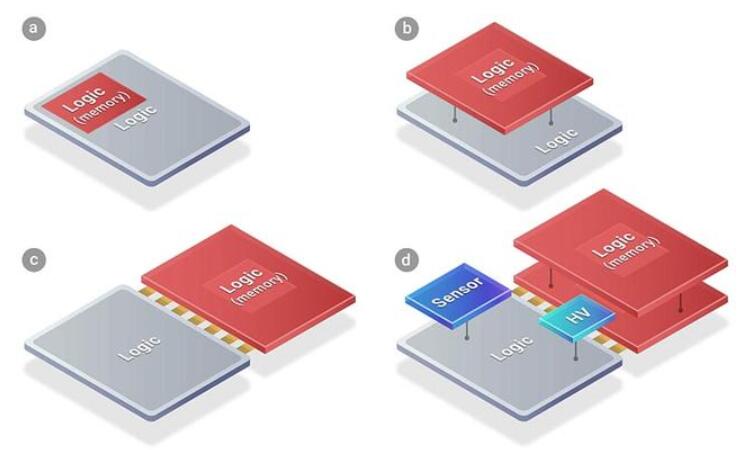
▲a is the SoC before chip splitting; b, c, d are the various partitioned chiplets and reintegration schemes supported by TSMC’s SoIC service platform
Through the use of TSV technology, TSMC’s SoIC technology can achieve a bump-free bonding structure, so that small chips of different sizes, processes, and materials can be reintegrated into an integrated chip similar to SoC, making the final integrated chip The area is smaller, and the system performance is better than the original SoC.
TSMC's back-end technologies, including CoWoS (Chip on Wafer on Substrate) and InFO (Integrated Fan-out) series packaging technologies, have been widely implemented. For example, this year's Fujitsu A64FX processor, which is ranked first in the world's TOP 500 supercomputer list, uses TSMC's CoWoS packaging technology, and the Apple mobile phone chip uses TSMC's InFO packaging technology.
In addition, TSMC has a number of specialized back-end fabs responsible for assembling and testing silicon chips, including 3D stacked chips, and processing them into packaged devices.
A major benefit of this is that customers can use more mature and lower-cost semiconductor technology on analog IO, RF and other modules that are not frequently changed and have little scalability, and use the most advanced semiconductor technology in core logic design. , Which not only saves costs, but also shortens the time to market for new products.
TSMC 3DFabric integrates advanced logic and high-speed storage devices into package modules. Under a given bandwidth, the wide interface of high bandwidth memory (HBM) enables it to run at a lower clock speed, thereby reducing power consumption.
If you look at the scale of the data center, the cost savings of these logic and HBM devices is considerable.
3. Intel uses the "decomposition design" strategy to achieve differentiated advantages
Similar to TSMC, Intel has already deployed advanced packaging technologies in multiple dimensions in the packaging field.
On the Intel Architecture Day 2020 on August 13, Intel announced a new hybrid integrated (Integrated Fan-out) technology. Test chips using this technology have been taped out in the second quarter of 2020.
Compared with the thermocompression bonding technology used in most packaging technologies, the hybrid bonding technology can reduce the bump pitch to less than 10 microns, providing higher interconnection density, higher bandwidth and lower power.
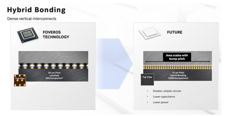
▲Intel Hybrid Technology
Intel has previously introduced standard packaging, 2.5D embedded multi-interconnect bridge (EMIB) technology, 3D package Foveros technology, Co-EMIB technology that combines EMIB and Foveros, omni-directional interconnect (ODI) technology and multi-mode I/ O (MDIO) technology, etc., after these package interconnection technologies are superimposed on each other, they can bring greater scalability and flexibility.
According to Song Jiqiang, Dean of Intel Research Institute, “The development of packaging technology is like building a house. At first, we built a single room, then built a courtyard, and finally reached a high-rise building. For Foveros 3D, what it achieves is When building high-rise buildings, the line can transmit at low power and high speed at the same time."
He believes that Intel's advantage in packaging technology is that it can know earlier how the house will be built in the future, which means that it can better design future chips.
Facing the future trend of heterogeneous computing, Intel has launched a "Digression design" strategy, combining new design methods and advanced packaging technologies to split key architecture components into individual chips that are still in a unified package.
That is to say, the original whole SoC chip is "divided into parts", first made into several parts such as CPU, GPU, I/O, etc., and then the fine-grained SoC is further improved, and the previous combination of functions is combined The idea is to switch to a combination of chip IP.
The advantage of this idea is that it can not only improve the efficiency of chip design and reduce the time for productization, but also effectively reduce the number of bugs caused by previous complex designs.
"The original solution that must be put on one chip can now be converted into multiple chips. In addition, not only Intel's multi-node process technology can be used, but also the partner's technology can be used." Song Jiqiang explained.
After these disassembled small parts are integrated, they are fast, have sufficient bandwidth, and can achieve low power consumption at the same time, and they have great flexibility, which will become a major difference advantage for Intel.
Fourth, Samsung's first 3D packaging technology can be used for 7nm process
In addition to TSMC and Intel, Samsung is also accelerating the deployment of its 3D packaging technology.
On August 13, Samsung also announced that its 3D packaging technology is "eXtended-Cube", or "X-Cube" for short, which is interconnected via TSV and can be used in 7nm or even 5nm processes.
According to Samsung, its X-Cube test chip can stack the SRAM layer on the logic layer and separate the SRAM from the logic part, thereby freeing up more space to stack more memory.
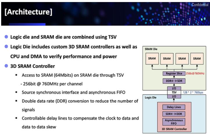
▲Samsung X-Cube test chip architecture
In addition, TSV technology can greatly shorten the signal distance between dies, increase data transmission speed and reduce power consumption.
Samsung said that the 3D packaging technology has achieved a major leap in speed and efficiency, and will help meet the stringent performance requirements of cutting-edge applications such as 5G, AI, AR, VR, HPC, mobile and wearable devices.
Conclusion: The three major chip giants attack advanced packaging
It can be seen that in 2020, the war on 3D packaging technology continues to escalate, and the three advanced chip manufacturers, TSMC, Intel, and Samsung, have increased their codes to explore a broader space for chip innovation.
Although the core details of these technical methods are different, they all lead to the same goal, all in order to continue to increase chip density and achieve more complex and flexible system-level chips to meet the increasingly diverse application needs of customers.
As the process technology approaches its limits and application requirements continue to diversify, in the future, chip manufacturers will not only solve technical challenges such as heat dissipation, but also hope to promote the integration of advanced packaging technologies from different manufacturers.