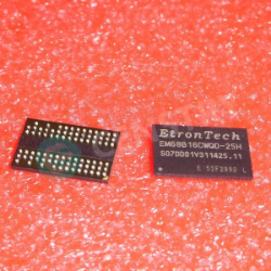
DDR2 32Mx16 PC800


圖片僅供參考.
有關產品詳細信息,請參閱產品規格。
DDR2 32Mx16 PC800
訂單滿$200即可獲贈限量版中式禮品一份.
訂單金額超過1000 美元可減免30 美元運費.
超過5000 美元的訂單可免運費和交易費.
這些優惠適用於新客戶和現有客戶,有效期為2024年1月1日至2024年12月31日.
Etron
EM68B16CWQH-25H datasheet
FBGA-84
記憶體
現在提交您的報價請求,我們期望在 4月 30, 2024內提供報價。現在就下訂單,我們期望在 5月 03, 2024內完成交易。時間是格林威治標準時間+8:00。


• JEDEC Standard Compliant
• JEDEC standard 1.8V I/O (SSTL_18-compatible)
• Power supplies: VDD & VDDQ = +1.8V ± 0.1V
• Operating temperature: TC = 0~85°C
• Supports JEDEC clock jitter specification
• Fully synchronous operation
• Fast clock rate: 333/400/533MHz
• Differential Clock, CK & CK#
• Bidirectional single/differential data strobe
- DQS & DQS#
• 4 internal banks for concurrent operation
• 4-bit prefetch architecture
• Internal pipeline architecture
• Precharge & active power down
• Programmable Mode & Extended Mode registers
• Posted CAS# additive latency (AL): 0, 1, 2, 3, 4, 5, 6
• WRITE latency = READ latency - 1 tCK
• Burst lengths: 4 or 8
• Burst type: Sequential / Interleave
• DLL enable/disable
• Off-Chip Driver (OCD)
- Impedance Adjustment
- Adjustable data-output drive strength
• On-die termination (ODT)
• RoHS compliant
• Auto Refresh and Self Refresh
• 8192 refresh cycles / 64ms
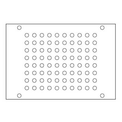
• 84-ball 8x12.5x1.2mm (max) FBGA
- Pb and Halogen Free
Description:
Overview The EM68B16C is a high-speed CMOS DoubleData-Rate-Two (DDR2), synchronous dynamic randomaccess memory (SDRAM) containing 512 Mbits in a 16- bit wide data I/Os. It is internally configured as a quad bank DRAM, 4 banks x 8Mb addresses x 16 I/Os. The device is designed to comply with DDR2 DRAM key features such as posted CAS# with additive latency, Write latency = Read latency -1, Off-Chip Driver (OCD) impedance adjustment, and On Die Termination(ODT). All of the control and address inputs are synchronized with a pair of externally supplied differential clocks. Inputs are latched at the cross point of differential clocks (CK rising and CK# falling). All I/Os are synchronized with a pair of bidirectional strobes (DQS and DQS#) in a source synchronous fashion. The address bus is used to convey row, column, and bank address information in RAS #, CAS# multiplexing style. Accesses begin with the registration of a Bank Activate command, and then it is followed by a Read or Write command. Read and write accesses to the DDR2 SDRAM are 4 or 8-bit burst oriented; accesses start at a selected location and continue for a programmed number of locations in a programmed sequence. Operating the four memory banks in an interleaved fashion allows random access operation to occur at a higher rate than is possible with standard DRAMs. An auto precharge function may be enabled to provide a self-timed row precharge that is initiated at the end of the burst sequence. A sequential and gapless data rate is possible depending on burst length, CAS latency, and speed grade of the device.

WQ: indicates 8x12.5x1.2mm (max) FBGA package
H: indicates Generation Code
H*: indicates Pb and Halogen Free

Request a quote EM68B16CWQH-25H at censtry.com. All items are new and original with 365 days warranty! The excellent quality
and guaranteed services of EM68B16CWQH-25H in stock for sale, check stock quantity and pricing,
view product specifications, and order contact us:sales@censtry.com.
The price and lead time for EM68B16CWQH-25H depending on the quantity required, please send your request to us,
our sales team will provide you price and delivery within 24 hours, we sincerely look forward to cooperating with you.

Etron
4087 PCS
EM68C16CWQG-25IH .PDF
Etron
4892 PCS
EM68A16CBQC-25IH .PDF
Etron
3953 PCS
EM68B16CWQK-25IH .PDF
2024-04-29
GOOD SUPPLIER FROM 10 YEARS. THANKS
2024-04-29
Jim is a pleasure to work with.
2024-04-28
Received the product without any problem. Fast shipping and reasonable prices. I recommend this store.
2024-04-27
good company,thanks George
2024-04-26
Great company. Quality product.
2024-04-22
Good parts, Great Service, pleasure to work with.
2024-04-16
Good supplier.
2024-04-02
Received the product without any problem. Fast shipping and reasonable prices. I recommend this store.
2024-03-07
Great company to work with! Smooth cooperation!
2024-01-13
Great Company, quick payment
我們高度重視您的回饋意見。 請分享您最真實的評價。
*請在發表評論之前登入您的帳戶