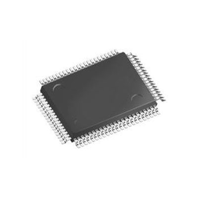
IC OSC SGL TIMER 2.1MHZ 8-SOIC


圖片僅供參考.
有關產品詳細信息,請參閱產品規格。
IC OSC SGL TIMER 2.1MHZ 8-SOIC
訂單滿$200即可獲贈限量版中式禮品一份.
訂單金額超過1000 美元可減免30 美元運費.
超過5000 美元的訂單可免運費和交易費.
這些優惠適用於新客戶和現有客戶,有效期為2024年1月1日至2024年12月31日.
TI
TLC555QDR datasheet
SOP-8
IC芯片
 Lead free/RoHS Compliant
現在提交您的報價請求,我們期望在 5月 03, 2024內提供報價。現在就下訂單,我們期望在 5月 08, 2024內完成交易。時間是格林威治標準時間+8:00。


TI
443 PCS
C3008A2 .PDF
TI
18 PCS
C16RCA/S4A26F17FNQ .PDF
TI
200 PCS
C16244AEP .PDF
TI
45 PCS
C138G086PZ .PDF
2024-05-02
Great company- no nonsense
2024-05-02
GREAT COMPANY!!! GREAT QUALITY!! GREAT SERVICE!
2024-05-01
Great Team!!
2024-05-01
Great parts , great price , great service.
2024-04-29
Great supplier over the year!!! we love Gil, Ed, and Karen there.......
2024-04-27
Haim is a great salesperson, one of the best around! Heather Fisher
2024-04-21
It is a pleasure doing business with Censtry.
2024-04-11
I hope we can do more buisness in the Future.
2024-03-20
It was a pleasure to work with Susan at Censtry. Thank you
2024-02-07
John Walsh is great to work and is very professional.
我們高度重視您的回饋意見。 請分享您最真實的評價。
*請在發表評論之前登入您的帳戶