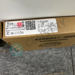
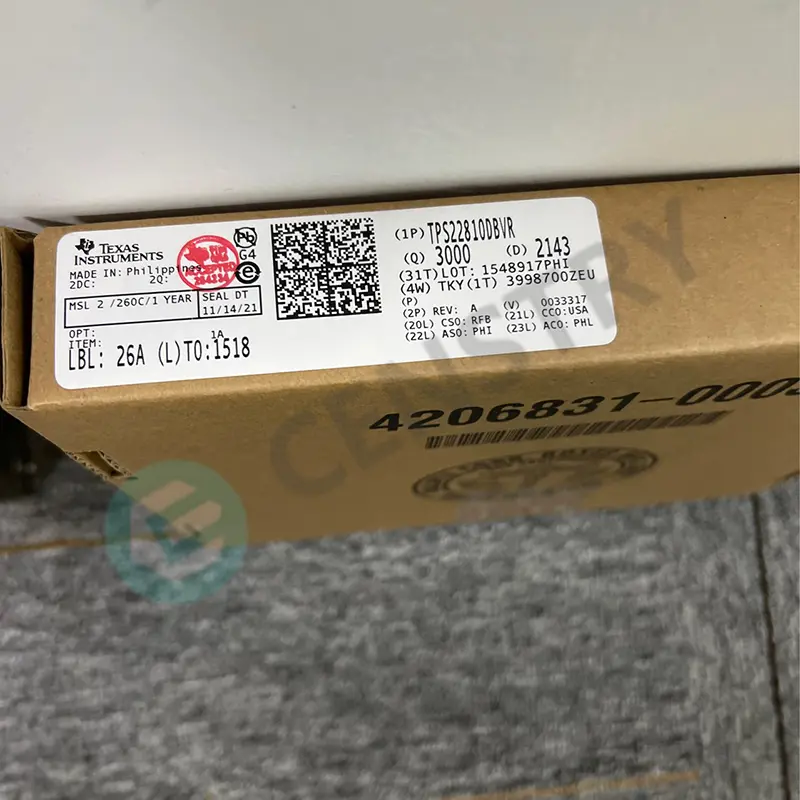
IC PWR SWITCH N-CHAN 1:1 SOT23-6


圖片僅供參考.
有關產品詳細信息,請參閱產品規格。
IC PWR SWITCH N-CHAN 1:1 SOT23-6
訂單滿$200即可獲贈限量版中式禮品一份.
訂單金額超過1000 美元可減免30 美元運費.
超過5000 美元的訂單可免運費和交易費.
這些優惠適用於新客戶和現有客戶,有效期為2024年1月1日至2024年12月31日.
TI
TPS22810DBVR datasheet
SOT-23-6
IC芯片
 Lead free/RoHS Compliant
現在提交您的報價請求,我們期望在 5月 03, 2024內提供報價。現在就下訂單,我們期望在 5月 07, 2024內完成交易。時間是格林威治標準時間+8:00。


1 Features
• Integrated Single Channel Load Switch
• Ambient Operating Temperature:
–40°C to +105°C
– SOT23-6 (DBV): 2-A Maximum Continuous Current 1
– WSON (DRV): 3-A Maximum Continuous Current 1
• Input Voltage Range: 2.7 V to 18 V
• Absolute Maximum Input Voltage: 20 V
• On-Resistance (RON)
– RON = 79 mΩ (typical) at VIN = 12 V
• Quiescent Current
– 62 µA (typical) at VIN = 12 V
• Shutdown Current
– 500 nA (typical) at VIN = 12 V
• Thermal Shutdown
• Undervoltage Lock-Out (UVLO)
• Adjustable Quick Output Discharge (QOD)
• Configurable Rise Time With CT Pin
• SOT23-6 Package
– 2.9-mm × 2.8-mm, 0.95-mm Pitch
1.45-mm Height (DBV)
• WSON Package
– 2-mm × 2-mm, 0.65-mm Pitch 0.75-mm Height (DRV)
• ESD Performance Tested per JESD 22
– ±2-kV HBM and ±1-kV CDM
(1) Thermal performance must be considered
2 Applications
• HD TV
• Industrial Systems
• Set Top Box
• Surveillance systems
3 Description
The TPS22810 is a single channel load switch with configurable rise time and with an integrated quick output discharge (QOD). In addition, the device features thermal shutdown to protect the device against high junction temperature. Because of this, safe operating area of the device is inherently ensured. The device contains an N-channel MOSFET that can operate over an input voltage range of 2.7 V to 18 V. SOT23-5 (DBV) package can support a maximum current of 2 A. WSON (DRV) package can support a maximum current of 3 A. The switch is controlled by an on and off input, which is capable of interfacing directly with low-voltage control signals.
The configurable rise time of the device greatly reduces inrush current caused by large bulk load capacitances, thereby reducing or eliminating power supply droop. Undervoltage lock-out is used to turn off the device if the VIN voltage drops below a threshold value, ensuring that the downstream circuitry is not damaged by being supplied by a voltage lower than intended. The configurable QOD pin controls the fall time of the device to allow design flexibility for power down.
The TPS22810 is available in a leaded, SOT-23 package (DBV) which allows to visually inspect solder joints, as well as a WSON package (DRV). The device is characterized for operation over the free-air temperature range of –40˚C to +105˚C.

Request a quote TPS22810DBVR at censtry.com. All items are new and original with 365 days warranty! The excellent quality
and guaranteed services of TPS22810DBVR in stock for sale, check stock quantity and pricing,
view product specifications, and order contact us:sales@censtry.com.
The price and lead time for TPS22810DBVR depending on the quantity required, please send your request to us,
our sales team will provide you price and delivery within 24 hours, we sincerely look forward to cooperating with you.
TI
443 PCS
C3008A2 .PDF
TI
18 PCS
C16RCA/S4A26F17FNQ .PDF
TI
200 PCS
C16244AEP .PDF
TI
45 PCS
C138G086PZ .PDF
2024-05-02
Excellent fast postage
2024-05-01
Ware dankend erhalten!
2024-05-01
Tested ALL OK!!!
2024-05-01
Excellent ***** Highly recommended - Thank you.
2024-04-30
Worked like a charm... thanks
2024-04-28
Llegó bien
2024-04-24
Would use Iceberg again. Good response to enquiry and requests.
2024-04-16
Great! recommended !
2024-03-31
We are very pleased with our business with her, and look to give her every PO we can. Thanks Dusty.
2024-02-28
Very reliable and delivered as promised. Mark and Wendy, great job! Thanks again.

我們高度重視您的回饋意見。 請分享您最真實的評價。
*請在發表評論之前登入您的帳戶