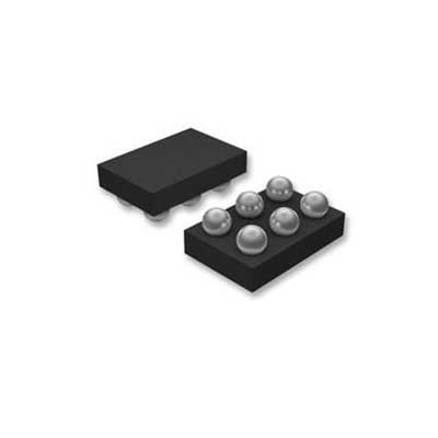
Power Switch/Driver 1:1 N-Channel 3A 6-DSBGA


圖片僅供參考.
有關產品詳細信息,請參閱產品規格。
Power Switch/Driver 1:1 N-Channel 3A 6-DSBGA
訂單滿$200即可獲贈限量版中式禮品一份.
訂單金額超過1000 美元可減免30 美元運費.
超過5000 美元的訂單可免運費和交易費.
這些優惠適用於新客戶和現有客戶,有效期為2024年1月1日至2024年12月31日.
TI
TPS22925CNYPHR datasheet
DSBGA-6
射頻集成電路
 Lead free/RoHS Compliant
現在提交您的報價請求,我們期望在 5月 06, 2024內提供報價。現在就下訂單,我們期望在 5月 08, 2024內完成交易。時間是格林威治標準時間+8:00。


1 Features
• Input Voltage Range: 0.65 V to 3.6 V
• On-Resistance
– RON = 9.2 mΩ at VIN = 3.6 V
– RON = 9.2 mΩ at VIN = 1.8 V
– RON = 10.2 mΩ at VIN = 1 V
– RON = 13.1 mΩ at VIN = 0.65 V
• 3-A Maximum Continuous Switch Current
• Quiescent Current, IQ,VIN = 29 µA at VIN = 3.6 V
• Low Control Input Threshold Enables 1.5-, 1.8-, 2.5-, or 3.3-V Logic
• Controlled Slew Rate
– tR = 97 µs at VIN = 3.6 V (TPS22925Bx)
– tR = 810 µs at VIN = 3.6 V (TPS22925Cx)
• Reverse Current Blocking (When Disabled)
• Quick Output Discharge (QOD) (TPS22925B and TPS22925C only)
• Wafer Chip Scale Package:
– 0.9 mm x 1.4 mm, 0.5-mm Pitch, 0.4-mm Height
• ESD Performance Tested per JESD 22
– 2-kV HBM and 1-kV CDM
2 Applications
• Computing
• SSD
• Tablets
• Wearables
• EPOS
3 Description
The TPS22925 product family consists of four devices: TPS22925B, TPS22925BN, TPS22925C,
and TPS22925CN. Each device is a 9-mΩ, singlechannel load switch with a controlled slew rate.
The devices contain an N–channel MOSFET that can operate over an input voltage range of 0.65 V to 3.6 V and can support a maximum continuous current of 3 A. This continuous current enables the devices to be used across multiple designs and end equipments. Each of the TPS22925 devices provides reverse current blocking when disabled allowing for power supply protection and power multiplexing capabilities.
The controlled rise time for the device greatly reduces inrush current caused by large bulk load capacitances, thereby reducing or eliminating power supply droop. When operating with an input voltage of 3.6 V, the TPS22925Bx devices feature a 97 μs rise time and the TPS22925Cx devices feature an 810 μs rise time.
The TPS22925 family of devices can help reduce the total solution size by offering an optional integrated, 150-Ω pull–down resistor for quick output discharge (QOD) when the switch is turned off. Each of the TPS22925 devices is available in a 0.9 mm × 1.4 mm, 0.5-mm pitch, 0.4-mm height 6–pin wafer chip scale package (WCSP) allowing for smaller, more integrated designs. The WCSP and 9 mΩ of onresistance allow use in space constrained, battery powered applications. The device is characterized for operation over the free–air temperature range of –40°C to +105°C.

Request a quote TPS22925CNYPHR at censtry.com. All items are new and original with 365 days warranty! The excellent quality
and guaranteed services of TPS22925CNYPHR in stock for sale, check stock quantity and pricing,
view product specifications, and order contact us:sales@censtry.com.
The price and lead time for TPS22925CNYPHR depending on the quantity required, please send your request to us,
our sales team will provide you price and delivery within 24 hours, we sincerely look forward to cooperating with you.
Adesto
7871 PCS
AT45DB641E-MHN-Y .PDF
Adesto
7327 PCS
AT25DF641A-MH-Y .PDF
GigaDevice
5386 PCS
GD9FS1G8F2AMGI .PDF
GigaDevice
7082 PCS
GD5F1GQ4UEYIGR .PDF
2024-05-04
They are very good goods. Thank you!!
2024-05-04
Fast and good as always, thanks!
2024-05-03
Excelent! Everything arrived OK!
2024-05-02
Very fast! Thank you!
2024-04-30
tested, everything ok
2024-04-25
Todo excelentemente bien
2024-04-16
Worked with Matt on first order with firm and found him to be responsive and professional. The company is a pleasure to do business and we will be back again for another deal. Thank you Matt for working with us and insuring our order processed smoothly.
2024-03-28
We have done several deals with Paul over the past 2 years Always a promt reply, friendly service, fast delivery, never a problemwith the quality of the parts.
2024-02-20
Waterlily has sold me a NAIS part 100pcs were perfect,The communication was easy and delivery was on time. We would using them again.
2023-12-07
very professional service . thank you Miss Kelley (eeparts in Shenzhen office ) Thank you for your support . we would like to purchased more electronics components from Miss Kelley . Hope more business each other further

我們高度重視您的回饋意見。 請分享您最真實的評價。
*請在發表評論之前登入您的帳戶