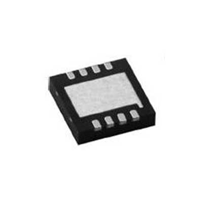
Power Switch/Driver 1:1 N-Channel 4A 8-WSON (2x2)


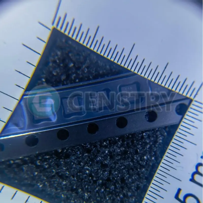
圖片僅供參考.
有關產品詳細信息,請參閱產品規格。
Power Switch/Driver 1:1 N-Channel 4A 8-WSON (2x2)
訂單滿$200即可獲贈限量版中式禮品一份.
訂單金額超過1000 美元可減免30 美元運費.
超過5000 美元的訂單可免運費和交易費.
這些優惠適用於新客戶和現有客戶,有效期為2024年1月1日至2024年12月31日.
TI
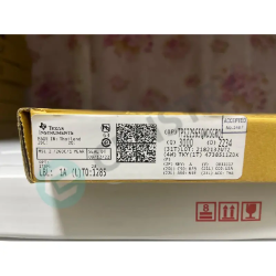
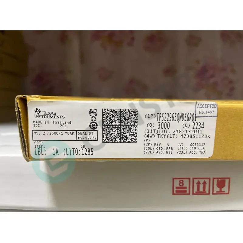
TPS22965QWDSGRQ1 datasheet
WSON-8
射頻集成電路
 Lead free/RoHS Compliant
現在提交您的報價請求,我們期望在 5月 04, 2024內提供報價。現在就下訂單,我們期望在 5月 08, 2024內完成交易。時間是格林威治標準時間+8:00。


1 Features
• Qualified for automotive applications
– AEC-Q100 qualified
– Device temperature grade 2: –40°C to +105°C
(TPS22965-Q1, TPS22965N-Q1)
– Device temperature grade 1: –40°C to +125°C
(TPS22965W-Q1, TPS22965NW-Q1)
– Device HBM ESD classification level 3A
– Device CDM ESD classification level C6
• Functional Safety-Capable
– Documentation available to aid functional safety system design
• Integrated single channel load switch
• Input voltage range: 0.8 V to 5.5 V
• Ultra-low on resistance (RON)
– RON = 16 mΩ at VIN = 5 V (VBIAS = 5 V)
– RON = 16 mΩ at VIN = 3.6 V (VBIAS = 5 V)
– RON = 16 mΩ at VIN = 1.8 V (VBIAS = 5 V)
• 4-A maximum continuous switch current
• Low quiescent current (50 µA)
• Low control input threshold enables use of 1.2-, 1.8-, 2.5- and 3.3-V logic
• Configurable rise time
• Quick Output Discharge (QOD) (TPS22965-Q1 and TPS22965W-Q1 only)
• WSON 8-pin package with thermal pad
2 Applications
• Automotive electronics
• Infotainment
• ADAS (Advanced Driver Assistance Systems)
3 Description
The TPS22965x-Q1 is a small, ultra-low-RON, singlechannel load switch with controlled turn-on. The device contains an N-channel MOSFET that can operate over an input voltage range of 0.8 V to 5.5 V and can support a maximum continuous current of 4 A. The VOUT rise time is configurable so that
inrush current can be reduced. The TPS22965-Q1 and TPS22965W-Q1 devices include a 225-Ω on-chip
load resistor for quick output discharge when the switch is turned off.
The TPS22965x-Q1 devices are available in a small, space-saving 2-mm × 2-mm 8-pin WSON package (DSG0008A) with integrated thermal pad allowing for high power dissipation. The TPS22965-Q1 and TPS22965N-Q1 devices are characterized for operation over the free-air temperature range of –40°C to 105°C. Furthermore, the TPS22965WQ1 and TPS22965NW-Q1 devices feature wettable flanks in the same WSON package (DSG0008B) and it is characterized for operation over the free-air temperature range of –40°C to +125°C.

Request a quote TPS22965QWDSGRQ1 at censtry.com. All items are new and original with 365 days warranty! The excellent quality
and guaranteed services of TPS22965QWDSGRQ1 in stock for sale, check stock quantity and pricing,
view product specifications, and order contact us:sales@censtry.com.
The price and lead time for TPS22965QWDSGRQ1 depending on the quantity required, please send your request to us,
our sales team will provide you price and delivery within 24 hours, we sincerely look forward to cooperating with you.
Adesto
7871 PCS
AT45DB641E-MHN-Y .PDF
Adesto
7327 PCS
AT25DF641A-MH-Y .PDF
GigaDevice
5386 PCS
GD9FS1G8F2AMGI .PDF
GigaDevice
7082 PCS
GD5F1GQ4UEYIGR .PDF
2024-05-03
It is a pleasure doing business with Censtry.
2024-05-03
Good and trustable Company
2024-05-03
I trust this company, very good reputation.
2024-05-02
Good company, great customer services and honest. I look forward to working with you guys again :)
2024-05-02
Good credit!Nice partner!
2024-05-01
Great company. Quality product.
2024-04-30
GOOD SUPPLIER - A+
2024-04-27
Great and reliable company, pleasure to deal with Avi...thanks
2024-04-22
Great company to deal with, always a pleasure to do business with Bryan. Hope we can do more business in the future.
2024-04-11
Great Company, nice to work with.Thank you very much Imraan

我們高度重視您的回饋意見。 請分享您最真實的評價。
*請在發表評論之前登入您的帳戶