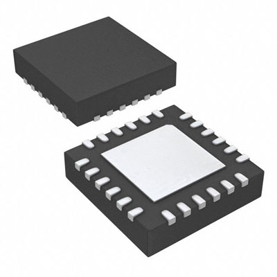
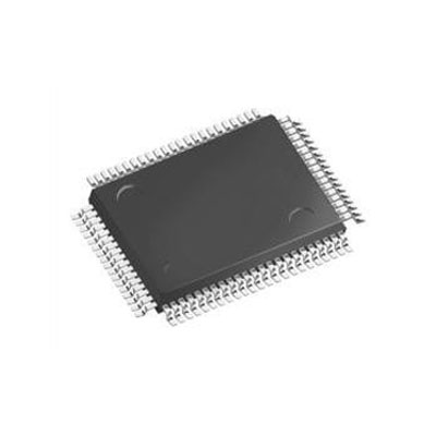
IC REG CONV DDR 1OUT 24WQFN


圖片僅供參考.
有關產品詳細信息,請參閱產品規格。
IC REG CONV DDR 1OUT 24WQFN
訂單滿$200即可獲贈限量版中式禮品一份.
訂單金額超過1000 美元可減免30 美元運費.
超過5000 美元的訂單可免運費和交易費.
這些優惠適用於新客戶和現有客戶,有效期為2024年1月1日至2024年12月31日.
TI
TPS54116QRTWRQ1 datasheet
WQFN-24
IC芯片
 Lead free/RoHS Compliant
現在提交您的報價請求,我們期望在 5月 06, 2024內提供報價。現在就下訂單,我們期望在 5月 09, 2024內完成交易。時間是格林威治標準時間+8:00。


1 Features
• AEC-Q100 Qualified With the Following Results:
– Device Temperature Grade 1: –40°C to +125°C Ambient Operating Temperature Range
– Device HBM ESD Classification Level 2
– Device CDM ESD Classification Level C6
• Single-chip DDR2, DDR3 and DDR3L Memory Power Solution
• 4-A Synchronous Buck Converter
– Integrated 33-mΩ High-side and 25-mΩ Lowside MOSFETs
– Fixed Frequency Current-mode Control
– Adjustable Frequency from 100 kHz to 2.5 MHz
– Synchronizable to an External Clock
– 0.6-V ±1% Voltage Reference Over Temperature
– Adjustable Cycle-by-Cycle Peak Current Limit
– Monotonic Start-up Into Pre-biased Outputs
• 1-A Source/Sink Termination LDO with ±20-mV DC Accuracy
– Stable with 2 × 10-µF MLCC Capacitor
– 10-mA Source/Sink Buffered Reference Output Regulated to Within 49% to 51% of VDDQ
• Independent Enable Pins with Adjustable UVLO and Hysteresis
• Thermal Shutdown
• -40°C to 150°C Operating TJ
• 24-pin, 4-mm x 4-mm WQFN Package
2 Applications
• DDR2, DDR3, DDR3L, and DDR4 Memory Power Supplies in Embedded Computing Systems
• SSTL_18, SSTL_15, SSTL_135, SSTL_12 and HSTL Termination
• Infotainment and Cluster
• Advanced Driver Assistance Systems (ADAS)
3 Description
The TPS54116-Q1 device is a full featured 6-V, 4-A, synchronous step down converter with two integrated MOSFETs and 1-A sink/source double data rate (DDR) VTT termination regulator with VTTREF
buffered reference output.
The TPS54116-Q1 buck regulator minimizes solution size by integrating the MOSFETs and reducing inductor size with up to 2.5-MHz switching frequency. The switching frequency can be set above the medium wave radio band for noise sensitive applications and is synchronizable to an external clock. Synchronous rectification keeps the frequency fixed across the entire output load range. Efficiency is maximized through integrated 25-mΩ low-side and 33-mΩ high-side MOSFETs. Cycle-by-cycle peak current limit protects the device during an overcurrent condition and is adjustable with a resistor at the ILIM pin to optimize for smaller inductors.
The VTT termination regulator maintains fast transient response with only 2 × 10-µF ceramic output capacitance reducing external component count. The TPS54116-Q1 uses remote sensing of VTT for best regulation.
Using the enable pins to enter a shutdown mode reduces supply current to 1-µA. Under voltage
lockout thresholds can be set with a resistor network on either enable pin. The VTT and VTTREF outputs
are discharged when disabled with ENLDO. Full integration minimizes the IC footprint with a small
4 mm × 4 mm thermally enhanced WQFN package

Request a quote TPS54116QRTWRQ1 at censtry.com. All items are new and original with 365 days warranty! The excellent quality
and guaranteed services of TPS54116QRTWRQ1 in stock for sale, check stock quantity and pricing,
view product specifications, and order contact us:sales@censtry.com.
The price and lead time for TPS54116QRTWRQ1 depending on the quantity required, please send your request to us,
our sales team will provide you price and delivery within 24 hours, we sincerely look forward to cooperating with you.
TI
443 PCS
C3008A2 .PDF
TI
18 PCS
C16RCA/S4A26F17FNQ .PDF
TI
200 PCS
C16244AEP .PDF
TI
45 PCS
C138G086PZ .PDF
2024-05-05
It is a gerat pleasure to work with Joanne
2024-05-05
JEFF IS THE HOOK-UP, GOOD SERVICE, LOW PRICES
2024-05-05
Keith and the staff at Censtry are a plessure to deal with, thank you for all your business. Chris
2024-05-05
Linda is the best and rocks. Thank you for your support. Hardy
2024-05-04
Mati and group are great to work with!
2024-05-04
Mr. Jordan, Quick, efficient, reliable seller !
2024-05-02
Nice smooth transaction
2024-04-30
One of the good companies in China to provide good quality, original parts. always pleasure dealing with
2024-04-24
as promised! Derek is professional!
2024-04-14
Pleasure to do business with, thank you

我們高度重視您的回饋意見。 請分享您最真實的評價。
*請在發表評論之前登入您的帳戶