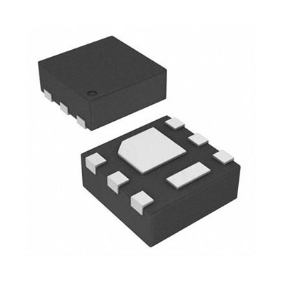
IC REG BOOST PROG 0.7A SYNC 6SON


圖片僅供參考.
有關產品詳細信息,請參閱產品規格。
IC REG BOOST PROG 0.7A SYNC 6SON
訂單滿$200即可獲贈限量版中式禮品一份.
訂單金額超過1000 美元可減免30 美元運費.
超過5000 美元的訂單可免運費和交易費.
這些優惠適用於新客戶和現有客戶,有效期為2024年1月1日至2024年12月31日.
TI
TPS61291DRVR datasheet
WSON-6
電源管理Ics
 Lead free/RoHS Compliant
現在提交您的報價請求,我們期望在 5月 03, 2024內提供報價。現在就下訂單,我們期望在 5月 08, 2024內完成交易。時間是格林威治標準時間+8:00。


1 Features
• Input Voltage Range 0.9V to 5V
• Startup Voltage 1.5V at 20mA Load
• Pin Selectable Output Voltages: 3.3V, 3V, 2.5V
• 15nA typical Quiescent Current in Bypass Mode
• 5.7μA typical Quiescent Current in Boost Mode
• Bypass Switch from VIN to VOUT
• IOUT > 200mA at 3.3V VOUT, VIN = 1.8V
• Internal Feedback Divider Disconnect (Bypass Mode)
• Controlled Bypass Transition Prevents Reverse Current into Battery
• Power-Save Mode at Light Loads
• Overtemperature Protection
• Redundant Overvoltage Protection
• Small 2mm x 2mm SON 6-pin package
2 Applications
• Metering (Gas, Water, Smart Meters)
• Remote Controls
• Home Security / Home Automation
• Single 3V Li-MnO2 or 2 x 1.5V Alkaline Cell Powered Applications
3 Description
The TPS61291 is a boost converter with pin selectable output voltages and an integrated bypass mode. In bypass operation, the device provides a direct path from the input to the system and allows a low power micro controller (MCU) such as the MSP430 to operate directly from a single 3V Li-MnO2 battery or dual alkaline battery cells.
In bypass mode the integrated feedback divider network for boost mode operation is disconnected from the output and the quiescent current consumption drops down to only 15nA (typical).
In boost mode the device provides a minimum output current of 200mA at 3.3V VOUT from 1.8V VIN. The boost mode is used for system components which require a regulated supply voltage and cannot directly operate from the input source. The boost converter is based on a current-mode controller using synchronous rectification to obtain maximum efficiency and consumes typically 5.7uA from the output. During startup of the boost converter, theVSEL pin is read out and the integrated feedback network sets the output voltage to 2.5V, 3V or 3.3V.
Bypass mode or boost mode operation is controlled by the system via the EN/BYP pin. The device integrates an enhanced bypass mode
control to prevent charge, stored in the output capacitor during boost mode operation, from flowing back to the input and charging the battery.
The device is packaged in a small 6-pin SON package (DRV) measuring 2.0mm × 2.0mm x 0.75mm.


Request a quote TPS61291DRVR at censtry.com. All items are new and original with 365 days warranty! The excellent quality
and guaranteed services of TPS61291DRVR in stock for sale, check stock quantity and pricing,
view product specifications, and order contact us:sales@censtry.com.
The price and lead time for TPS61291DRVR depending on the quantity required, please send your request to us,
our sales team will provide you price and delivery within 24 hours, we sincerely look forward to cooperating with you.
TI
443 PCS
C3008A2 .PDF
TI
18 PCS
C16RCA/S4A26F17FNQ .PDF
TI
200 PCS
C16244AEP .PDF
TI
45 PCS
C138G086PZ .PDF
2024-05-02
Excellent fast postage
2024-05-02
Ware dankend erhalten!
2024-05-02
Tested ALL OK!!!
2024-05-01
Excellent ***** Highly recommended - Thank you.
2024-05-01
Worked like a charm... thanks
2024-04-29
Llegó bien
2024-04-27
Would use Iceberg again. Good response to enquiry and requests.
2024-04-21
Great! recommended !
2024-04-11
We are very pleased with our business with her, and look to give her every PO we can. Thanks Dusty.
2024-03-20
Very reliable and delivered as promised. Mark and Wendy, great job! Thanks again.

我們高度重視您的回饋意見。 請分享您最真實的評價。
*請在發表評論之前登入您的帳戶