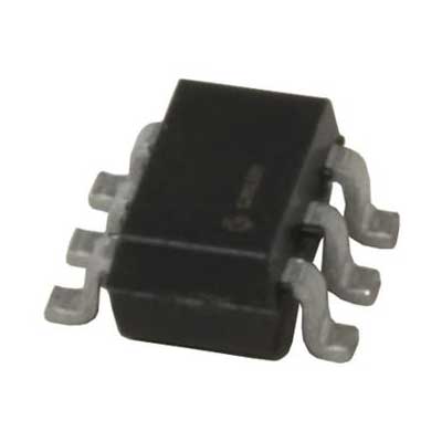
IC GATE DRVR LOW-SIDE SOT23-6


圖片僅供參考.
有關產品詳細信息,請參閱產品規格。
IC GATE DRVR LOW-SIDE SOT23-6
訂單滿$200即可獲贈限量版中式禮品一份.
訂單金額超過1000 美元可減免30 美元運費.
超過5000 美元的訂單可免運費和交易費.
這些優惠適用於新客戶和現有客戶,有效期為2024年1月1日至2024年12月31日.
TI
UCC27511DBVR datasheet
SOT23-6
IC芯片
 Lead free/RoHS Compliant
現在提交您的報價請求,我們期望在 5月 06, 2024內提供報價。現在就下訂單,我們期望在 5月 08, 2024內完成交易。時間是格林威治標準時間+8:00。


1FEATURES
• Low-Cost, Gate-Driver Device Offering Superior Replacement of NPN and PNP Discrete Solutions
• 4-A Peak Source and 8-A Peak Sink Asymmetrical Drive
• Strong Sink Current Offers Enhanced Immunity Against Miller Turn On
• Split Output Configuration (allows easy and independent adjustment of turn-on and turn- off speeds)
• Fast Propagation Delays (13-ns typical)
• Fast Rise and Fall Times (9-ns and 7-ns typical)
• 4.5-V to 18-V Single Supply Range
• Outputs Held Low During VDD UVLO (ensures glitch free operation at power-up and power-down)
• TTL and CMOS Compatible Input Logic Threshold, (independent of supply voltage)
• Hysteretic Logic Thresholds for High Noise Immunity
• Dual Input Design (choice of an inverting (IN-pin) or non-inverting (IN+ pin) driver configuration)
– Unused Input Pin can be Used for Enable or Disable Function
• Output Held Low when Input Pins are Floating
• Input Pin Absolute Maximum Voltage Levels Not Restricted by VDD Pin Bias Supply Voltage
• Operating Temperature Range of -40°C to 140°C
• 6-Pin DBV Package (SOT-23)
2 APPLICATIONS
• Switch-Mode Power Supplies
• DC-to-DC Converters
• Companion Gate Driver Devices for Digital Power Controllers
• Solar Power, Motor Control, UPS
• Gate Driver for Emerging Wide Band-Gap Power Devices (such as GaN)

3 DESCRIPTION
The UCC27511 single-channel, high-speed, low-side gate driver device is capable of effectively driving MOSFET and IGBT power switches. Using a design that inherently minimizes shoot-through current, UCC27511 is capable of sourcing and sinking high, peak-current pulses into capacitive loads offering rail-to-rail drive capability and extremely small propagation delay typically 13 ns.
The UCC27511 provides 4-A source, 8-A sink (asymmetrical drive) peak-drive current capability. Strong sink capability in asymmetrical drive boosts immunity against parasitic, Miller turn-on effect. The UCC27511 device also features a unique split output configuration where the gate-drive current is sourced through OUTH pin and sunk through OUTL pin. This unique pin arrangement allows the user to apply independent turn-on and turn-off resistors to the OUTH and OUTL pins respectively and easily control the switching slew rates. UCC27511 is designed to operate over a wide VDD range of 4.5 V to 18 V and wide temperature range of -40°C to 140°C. Internal Under Voltage Lockout (UVLO) circuitry on VDD pin holds output low outside VDD operating range. The capability to operate at low voltage levels such as below 5 V, along with best in class switching characteristics, is especially suited for driving emerging wide band-gap power switching devices such as GaN power semiconductor devices.

Request a quote UCC27511DBVR at censtry.com. All items are new and original with 365 days warranty! The excellent quality
and guaranteed services of UCC27511DBVR in stock for sale, check stock quantity and pricing,
view product specifications, and order contact us:sales@censtry.com.
The price and lead time for UCC27511DBVR depending on the quantity required, please send your request to us,
our sales team will provide you price and delivery within 24 hours, we sincerely look forward to cooperating with you.
TI
443 PCS
C3008A2 .PDF
TI
18 PCS
C16RCA/S4A26F17FNQ .PDF
TI
200 PCS
C16244AEP .PDF
TI
45 PCS
C138G086PZ .PDF
2024-05-05
Great company. Quality product.
2024-05-05
Honest & Reliable Company
2024-05-04
Fine company to work with
2024-05-04
Just did a large order with Censtry in China and they were excellent.
2024-05-03
I will give a 5 star.
2024-05-02
Good company to do business .
2024-04-29
Great company. Excellent prices and quality parts.
2024-04-24
Good supplier!!
2024-04-13
Good parts, excellent service, quick shipment. Thanks Katie and Nichole
2024-03-23
I recommend! Fast delivery and high quality product!

我們高度重視您的回饋意見。 請分享您最真實的評價。
*請在發表評論之前登入您的帳戶